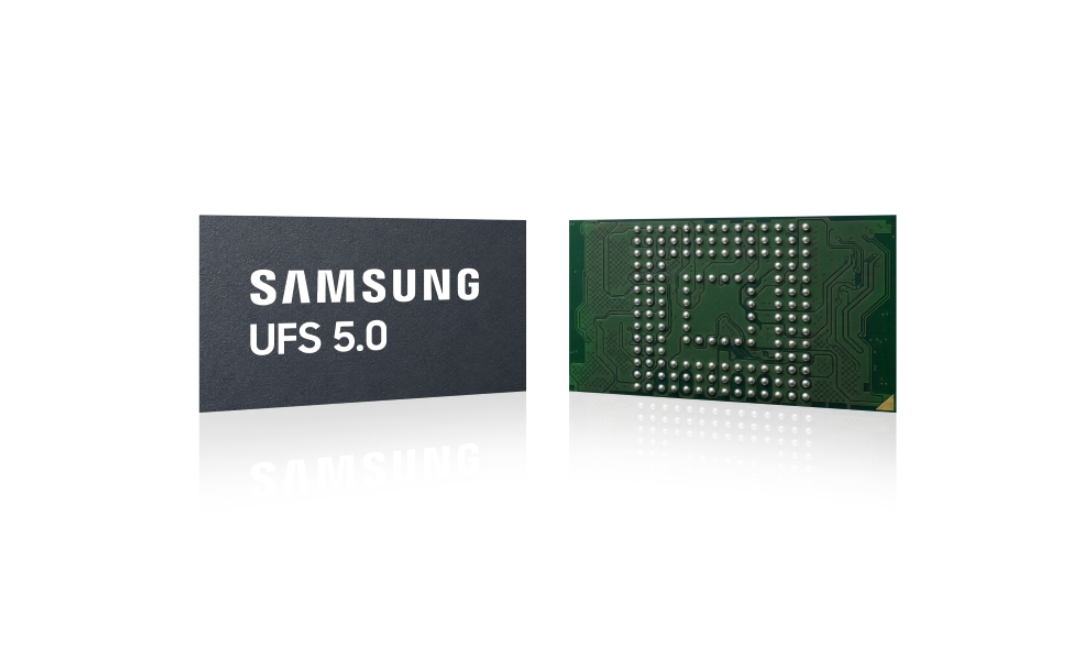
Smartphone and electronics giant Samsung recently announced that it’s been working on its latest Universal Flash Storage (UFS) 5.0 solution, which it says is designed to enable more capable and efficient AI services on future mobile devices. According to the company, the new memory technology greatly reduces latency and speeds up response times when running large language models (LLMs) directly on-device.
As such, UFS 5.0 uses the latest JEDEC embedded memory interface standard, which allows it to reach bandwidth speeds of up to 10.8 gigabytes per second, including a sequential read speed of up to 10.8 gbps, and a sequential write speed of up to 9.5 gbps, which is essentially twice as fast as the previous UFS 4.1 standard. Jangseok Choi, head of Memory Product Planning at Samsung comments:
In the era of on-device AI, storage devices are evolving into a key driver defining AI experiences… As we successfully move beyond the development stage of the industry’s first UFS 5.0 solution, Samsung is setting a new standard for storage on the go and will continue to drive innovation for the next-generation mobile platform market.
Beyond raw speed, the UFS 5.0 solution improves power efficiency by more than 40% compared to UFS 4.1. Samsung achieved this efficiency gain through innovations like clock gating and multi-voltage technologies, which significantly reduce the power required for data transfers and extend the battery life of upcoming mobile devices.
Samsung also designed its UFS 5.0 to be compact, measuring just 7.5mm x 13mm x 0.9mm—this allows for better design flexibility for hardware categories such as mobile, wearable, and even extended reality (XR) devices. Samsung plans to begin mass production of the UFS 5.0 solution in the fourth quarter of this year, offering a variety of storage capacities up to one terabyte (TB).